ELECTRONICS
QUALITY CONTROL


INTRODUCTION
• electronic components
• the printed circuit board

Figure 1: Electronic components
Electronic components are soldered onto the printed circuit board. This operation is called “brazing” which, unlike soldering, allows the components to be assembled without melting. Brazing only melts the filler metal, and that ensures continuity between the components.

Figure 2: Making a solder joint

Figure 3: Printed circuit board and illustration of metallised via holes


Figures 4 & 5: Electronic circuits
There are several categories of connectors: electrotechnical connectors (electrical sockets, power supply, terminals, terminal blocks or “dominoes”, etc.), electronic pins, computer connectors, audio (JACK, DIN, SPEAKON, etc.) and video connectors (HDMI, VGA, DVI, etc.) or so-called “professional” connectors (MIL-DTL- 38999, DBAS, BNC-TNC, etc.).

METALLOGRAPHIC PREPARATION
The main materials found in the field of electronics are:
• Metals with excellent electrical conductivity or coatings such as copper, silver, nickel and gold,
• Tin alloys for soldering,
• Polymers for printed circuit boards and electronic modules,
• The glass and ceramics (and silicon) that make up the various components.
Inspection requires metallographic preparation. Obtaining an inspection surface requires a succession of operations, each as important as the next, regardless of the material.
These steps are in the following order:
• The removal of the product to be examined (if necessary), called “CUTTING”.
• Standardisation of the geometry of the sample taken (if necessary), called “MOUNTING”.
• Improvement of the surface condition of this sample, called “POLISHING”.
• Characterisation of the sample: revealing the microstructure of the sample by an etching reagent (if necessary) called “METALLOGRAPHIC ETCHING” and microscopic observation (optical or electronic).

CUTTING
In other words, it is essential to avoid heating, deformation or excessive aggressiveness of the cut, which can lead to many different types of damage (cracks/spalling of components, detachment of coatings/metallisations, etc.) to the areas to be inspected. Cutting is a fundamental step which conditions the further preparation and inspection of parts.
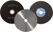
PRESI’s wide range of medium and large capacity cutting and micro-cutting machines, and also the range of WELL diamond wire saws, can be adapted to any need with regard to cutting precision, sizing or quantity of products to be cut:

The choice of machine type depends on the geometry of the workpieces to be cut and their sensitivity/fragility, as the clamping possibilities differ. The advantage of wire saws is that they use low support forces which are gentle on the specimens. They also provide very good surface finishes but have longer cutting times.
CLAMPING

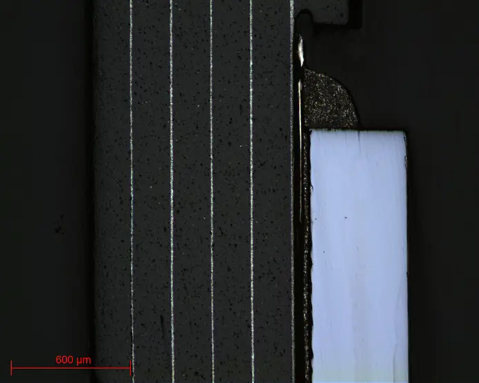
Figure 11: Example of clamping of an electronic circuit – FLEXICUT


Figures 12 & 13: Examples of clamping of an electronic circuit – FLEXICUT

Figure 14: Example of clamping a connector MECATOME T202

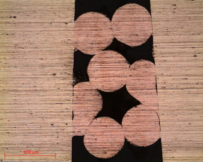
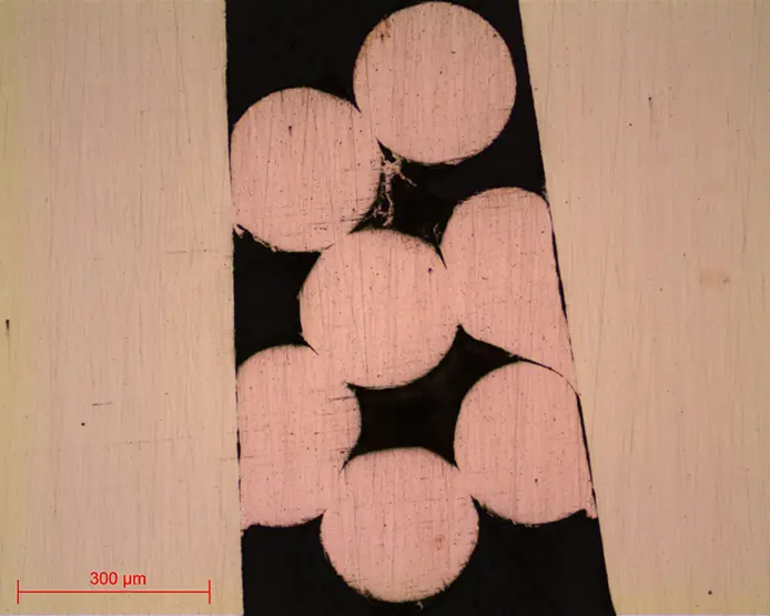
Figures 15 & 16: Examples of clamping and electronic connector 4000 series wire saw
CONSUMABLES
Wire saws, on the other hand, are used with a cutting fluid that acts as a lubricant and “cleaner” that extends the life of the wire and allows a better quality of cut to be achieved.
 |
SOFT METALS (Copper, Tin, Gold, Silver, etc.) | PLASTICS AND POLYMERS | CERAMICS |
| Micro-cutting | UTW S Ø180 |
UTW S Ø180 LM+ LR |
LM+ LR |
| Medium-capacity cutting | MNF T |
MNF LM+ LR |
LM+ LR |
Table 1: Choosing the right cut-off wheel type according to the main material of the electronic part
The consumables available for wire saws are stainless steel wires set with diamonds. The characteristics of the wires vary according to requirements and needs. The range is comprised of seven wire diameters from 0.1-0.7 mm and five diamond grit sizes from 20-64μm.

MOUNTING
=> Achieving good-quality mounting is essential to protect fragile materials and also to achieve good preparation results for polishing and future analysis.
There are two mounting options: hot or cold mounting. In electronics it is always preferable to use the cold mounting since very often the parts are fragile and therefore unsuitable for high pressures, and they are probably also sensitive to heat.
COLD MOUNTING
+ POINT
+ POINT
CONSUMABLES
 |
MICRO-ELECTRONICS CONNECTION TECHNOLOGY |
| Cold process | Pressurized acrylic KM-U Hot Epoxy IP MA2+ 2S* |
Table 2: Choosing the right mounting resin type
* Suitable for very large series
=> This resin has the advantage of a short curing time (15 minutes) and also presents very good hardness.

Figure 19: Coating with the use of “pressure coating equipment”

POLISHING
PRESI offers a wide range of manual and automatic polishing machines, with a wide choice of accessories, to cover all needs, from pre-polishing to super-finishing and polishing of single or series samples.
The aim of metallographic preparation of connector or microelectronic samples is often to reach and observe very precise areas of the parts. Therefore, polishing must be carried out in the most controlled manner possible. Manual polishing is therefore more advisable.
CONSUMABLES AND POLISHING RANGE
=> All the first steps of each range are called “levelling” and consist of removing material quickly to level the surface of the specimen (and resin). Those given below are standard and can therefore be modified as required. In practice, the aim is to reach the area of the sample to be studied after the pre-polishing steps. In this way the polishing is carried out directly on the components to be inspected.
Applied pressures vary according to sample size, but in general the following applies: 1daN per 10mm mounting diameter for the pre-polishing steps (ex: Ø40mm = 4 daN) then reduce force by 0.5daN at each polishing step with an abrasive suspension.
RANGE N°1
| N° | Support | Suspension / Lubricant | Platen Speed (RPM) | Head Speed (RPM) | Rotation direction platen / head | Time |
| 1 | SiC P320 | Ø / Water | 300 | 150 | 1’ | |
| 2 | SiC P1200 | Ø / Water | 300 | 150 | 1’ | |
| 3 | RAM | 3μm LDM / Reflex Lub | 150 | 135 | 3’ | |
| 4 | NT | 1μm LDM / Reflex Lub | 150 | 135 | 1’ | |
| 5 | SUPRA | (SPM) / Water | 150 | 100 | 1’ |
RANGE N°2
| N° | Support | Suspension / Lubricant | Platen Speed (RPM) | Head Speed (RPM) | Rotation direction platen / head | Time |
| 1 | Tissediam 40μm | Ø / Water | 300 | 150 | 2’ | |
| 2 | Tissediam 20μm | Ø / Water | 300 | 150 | 2’ | |
| 3 | TOP | 9μm LDP / Reflex Lub | 150 | 135 | 5’ | |
| 4 | RAM | 3μm LDP / Reflex Lub | 150 | 135 | 2’ | |
| 5 | SUPRA | SPM / Water | 150 | 100 | 2’ |
More generally, an “electronics” sample is made up of a multitude of different materials. There is therefore a risk of creating unevenness between the different components during polishing, causing difficulties during observation.
Sometimes, it is not necessary to carry out the polishing range up to super-finishing, particularly in the case of crimping controls, dimensioning or any other inspections on large connector samples.
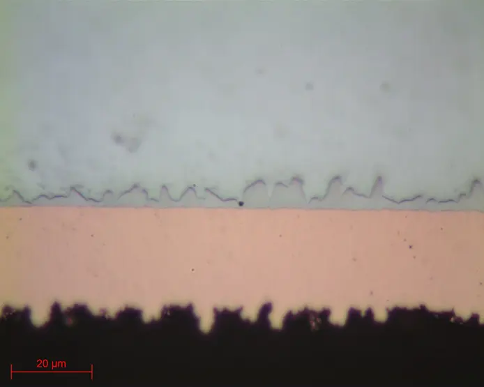
However finishing must be performed with colloidal silica in the last polishing stage to observe the finest components, intermetallics, porosity brazing, etc…

MICROSCOPY
Micrograph 1: Polished crimp up to 3μm lens x10
Micrograph 2: Polished crimp up to 1μm lens x10
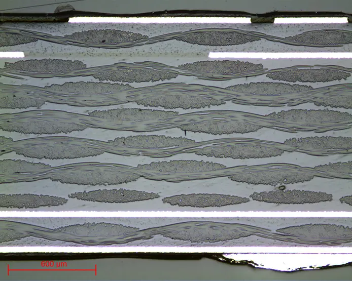
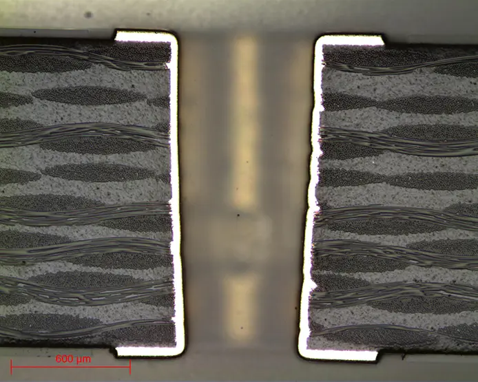
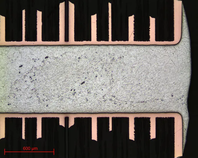
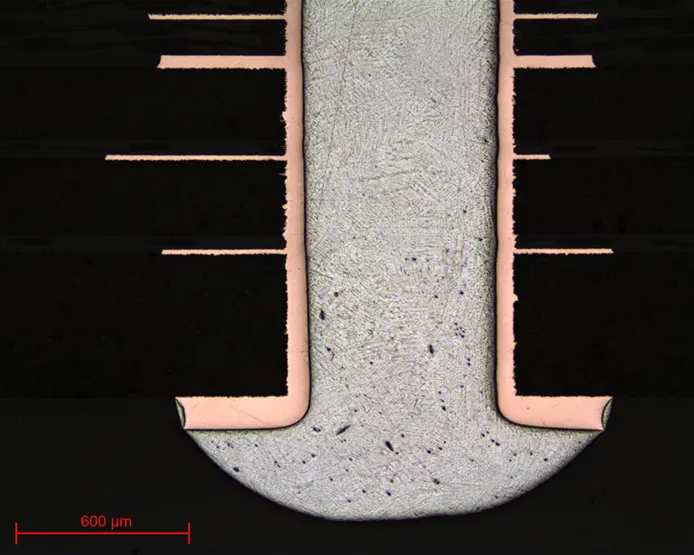
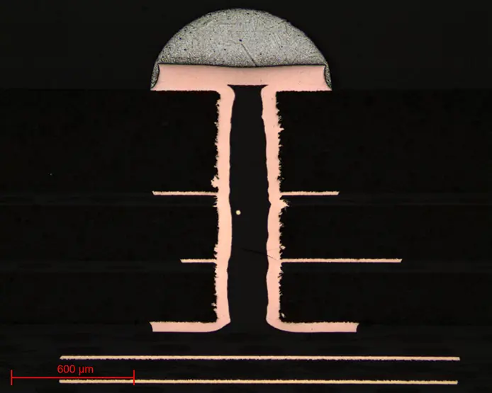
Micrographs 3 and 4: Polished circuit board up to SPM lens x5
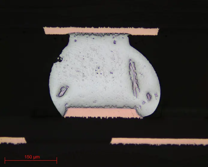
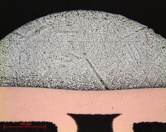
Micrograph 5: BGA solder polished to SPM lens x5
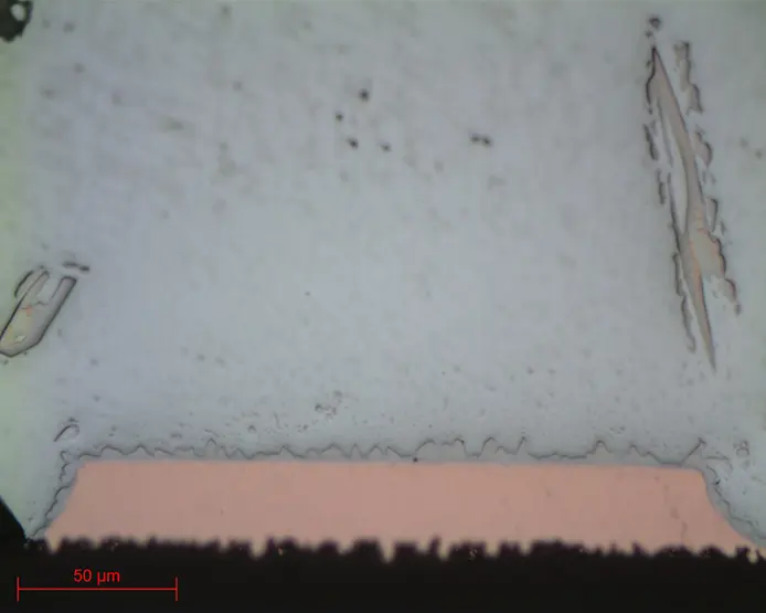
Micrograph 6: BGA solder polished up to SPM lens x20
Micrograph 7: BGA solder polished up to SPM lens x50
Micrograph 8: BGA solder polished to SPM lens x100
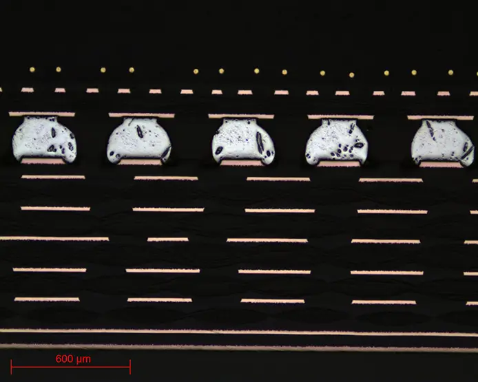
Micrograph 9: Polished solder up to SPM lens x5
Micrograph 10: Polished solder up to SPM lens x5
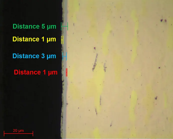
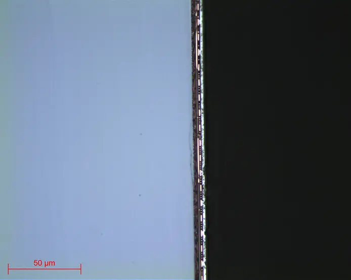
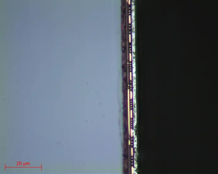
Micrographs 11 and 12: Brass with copper, nickel and gold plating polished up to SPM lens x100
Micrograph 13: Solder and metallization polished up to SPM lens x5
Micrograph 14: Solder and metallization polished up to SPM lens x20
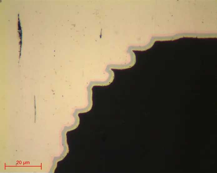
Micrograph 15: Ceramic component + polished silicon up to SPM lens x5
Micrograph 16: Ceramic component + polished silicon up to SPM lens x50
Micrograph 17: Ceramic component + polished silicon up to SPM lens x100
DOWNLOAD THE LAB'NOTE
Simply fill out the form below:
Discover our other Lab’Note:
- 3D printing quality control
- Hardened heat treatment control
- Medical device quality control
- Steel quality control
- Stainless steel quality control
- Cast iron quality control
- Copper alloy quality control
- Aluminum quality control
- Nickel quality control
- Titanium quality control
- Ceramic materials quality control
- Electronics quality control
- Precious metal quality control